Nowadays, photonics systems get more and more complex. Often, the required optical setup may require the size of a living room table. No doubt that will work and the desired tasks can be accomplished with such bulky systems. However, you certainly recognize that such a system of highly populated optical components is very difficult to industrialize and to scale up for mass production. So, what could be the solution?
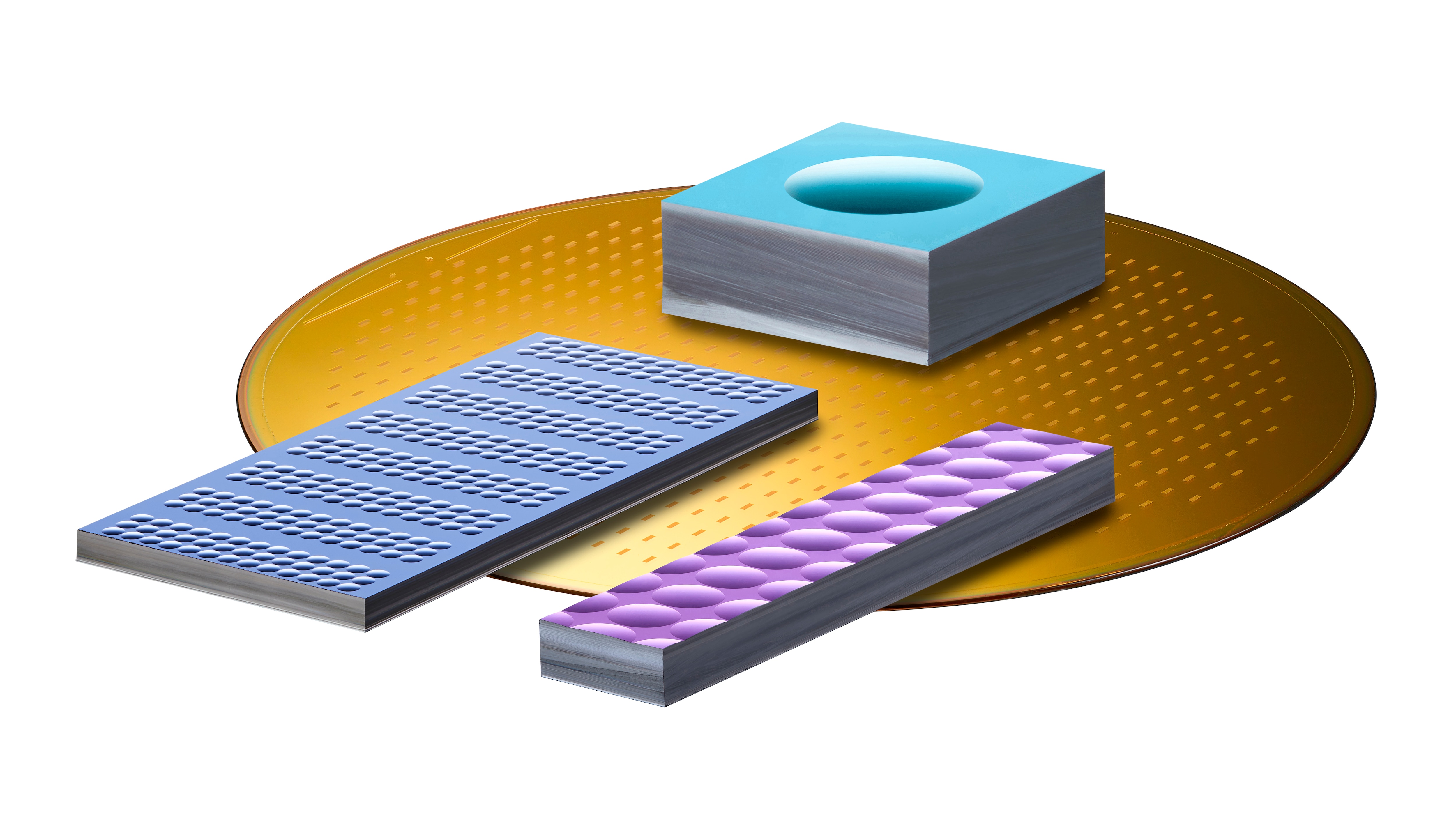
Photonic integrated circuits (PIC) seem to be the best approach among today's state-of-the-art options. When coupling light into- and out of the PIC or other forms of optical circuits, premium quality micro-lenses (shown in the first figure) can be also the best fit to maintaining high efficiency light coupling on one hand and vast scaling up to mass production requirements on the other.
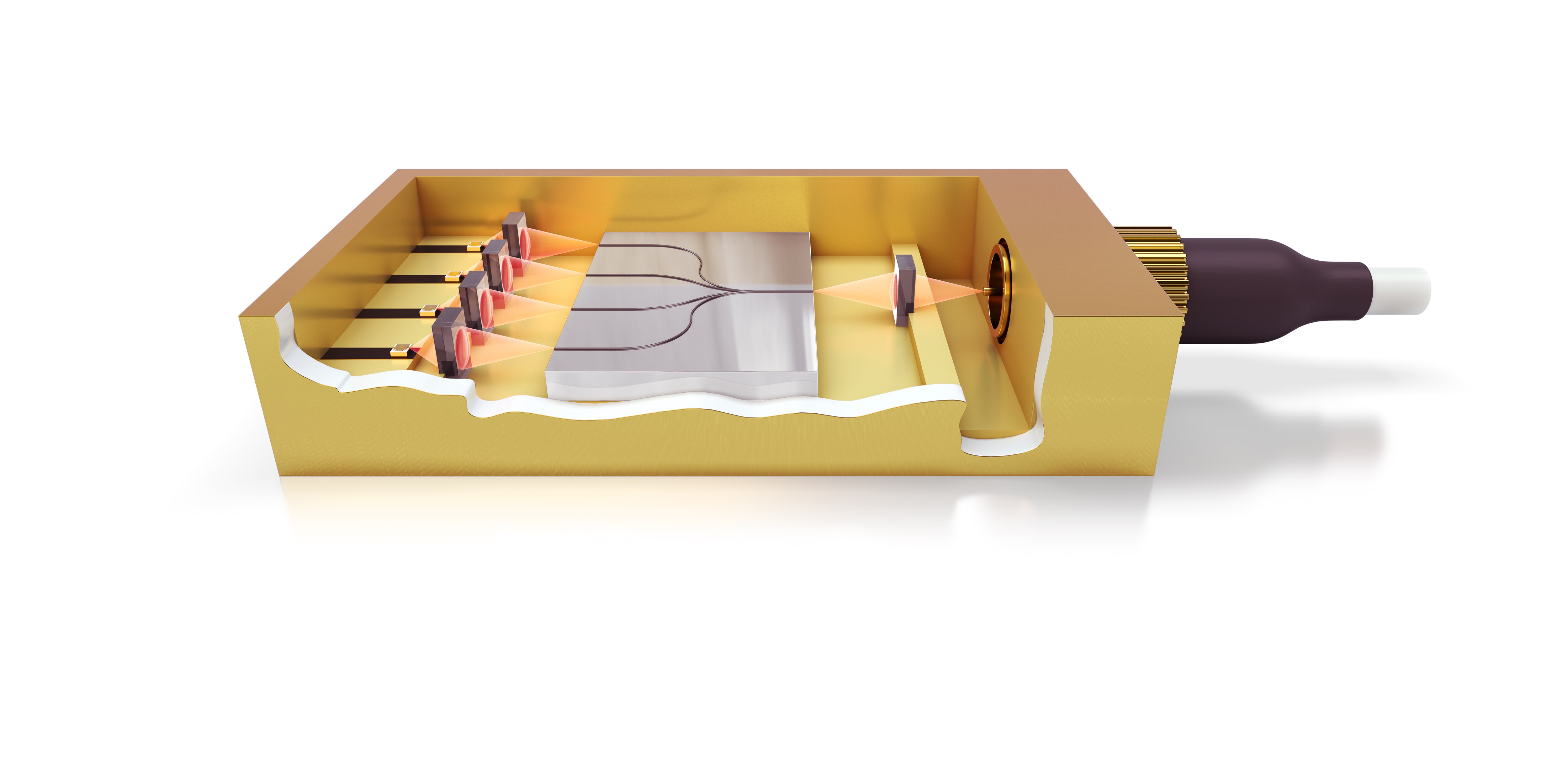
Silicon micro-lens chip of sub-millimeter dimension empowers those optical sub-assembly modules by coupling light from a laser diode into the optical circuit and further toward optical fibers, see in the second figure.
Such an assembly scheme can be adopted wherever PICs employed. For instance, frequency modulated continuous wave (FMCW) light detection and ranging (LIDAR) and Quantum applications need interferometers, splitting optical paths, branching them in multiple outputs.
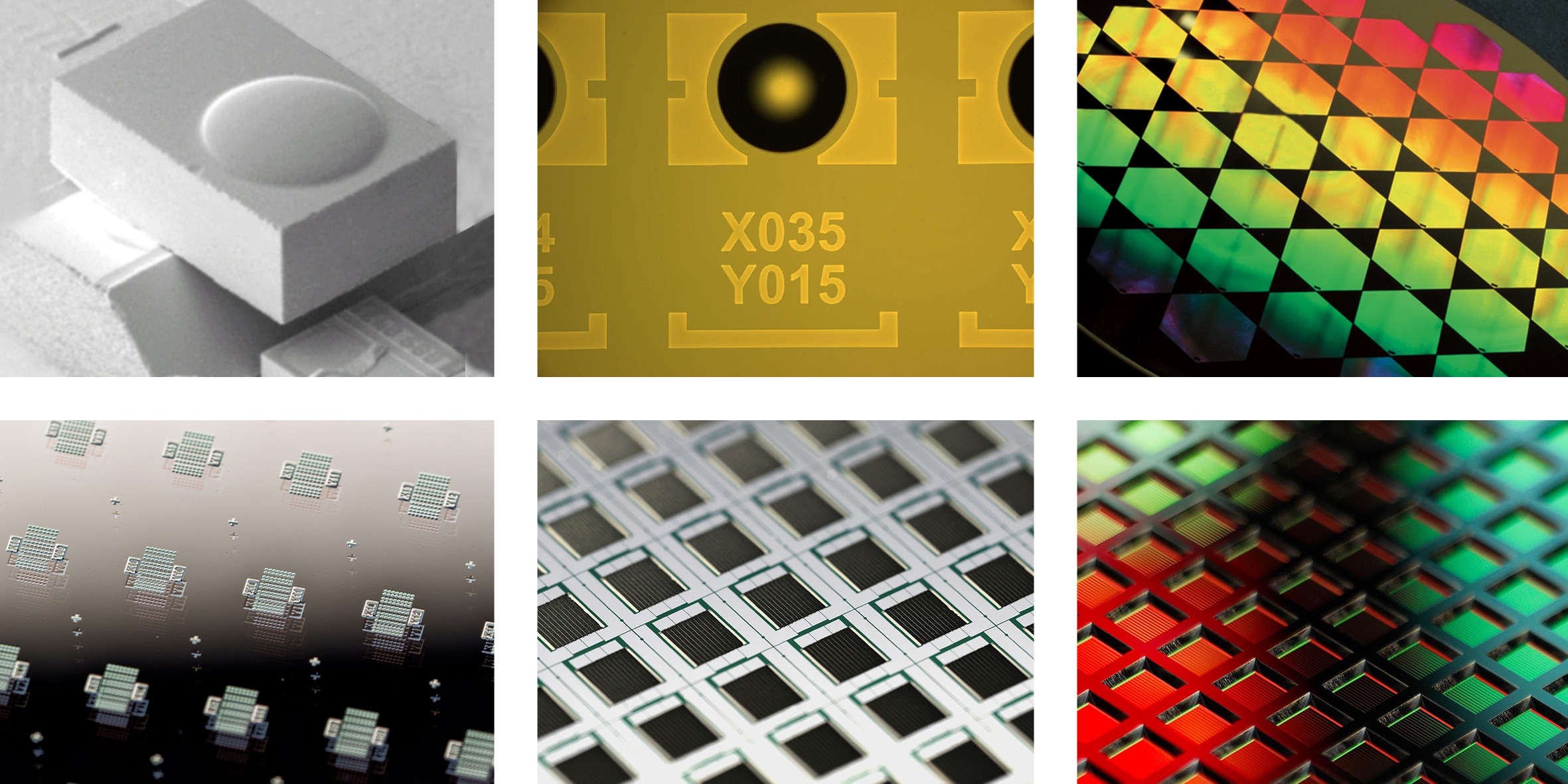
In addition to the optical characteristics, wafer-level MEMS processed micro-optics allow adding a wide range of mechanical structuring and metallization features to facilitate higher integration, smarter embedding and further miniaturization of optical sub-assemblies, see examples in the third figure.
Needless to mention that wafer-level micro-optics manufacturing is probably the smartest way to scale-up production output from prototype to multi-millions, exactly as PIC does.